DeMon — Debug + Monitor
AntOS host, system supervisor, hardware glue, and boot-UI display engine — pronounced "Demon".
DeMon is built around the RPi CM5 lite for the eZXSpectrum and RPi CM5 lite for the Ant64 (paired with an ESP32-C5 for wireless) and sits at the centre of everything: it boots the system, programs the FPGA, runs AntOS, watches over every other chip, drives the keyboard display via MIPI, sends a display image to the FPGA (FireStorm) via one HDMI and layer and other data via it's other HDMI. The PCIE 1x port gots to the serdes interface on the FPGA, it also provides hardware debugging across the entire Ant64.
The choice to host AntOS on DeMon — rather than on the FireStorm Execution Engine inside the FPGA — has one important consequence: AntOS keeps running while the FPGA is being reconfigured. Loading a personality cartridge, flashing a development bitstream, or recovering from a fault all happen without disturbing the OS. The main display blanks only for as long as the FPGA takes to reconfigure — a fraction of a second for the native chipset on a normal boot, somewhat longer for a personality load — and AntOS keeps running on DeMon throughout.
Overview
| Feature | Detail |
|---|---|
| Main chip | CM5 lite quad core ARM |
| RAM | 1 or 2GB expandable by swapping compute modules |
| Wireless chip | ESP32-C5 (Wi-Fi 6, Bluetooth 5.3, Thread, Zigbee) |
| RTC | Microchip MCP79410 |
| RTC battery | CR2450 — up to 20 years life |
| Storage | Internal HS USB hub — DBFS master (D:), DBFS shadow (D!:), internal general drive (B:), external memory-stick port (E:) · external SD card slot (A:), Cartridge (Ant64 only, C:) — see Storage below and Filesystem & Drive Letters for the full scheme |
| OS | AntOS runs here, on the CM5 |
| Display feed | MIPI DSI to a 4.3″ 480×800 IPS touch panel (ST7102, in-cell touch) in portrait, right of the keyboard where the numeric keypad would sit; 2× HDMI to FPGA (one for display overlay, the other for data sent in the video stream) |
| Audio | Triple SID engine (L/C/R) — 9 SID voices, in software · SAM speech synthesizer — formant TTS, in software · both streamed to FireStorm |
Why Cm4/5?
The move from the ESP32-P4 to a Raspberry Pi Compute Module is driven by four things (full rationale, trade-offs and open questions are in the CM5 supervisor design notes):
- The softraster ceiling disappears. The VideoCore GPU means AntOS's ImGui UI runs on the stock GLES backend and doesn't software-rasterise at all — the measured 35.7 ms/frame editor spike goes away, and with it the requirement that shaped FireStorm hardest (a texture sampler for the font atlas). The FPGA's primitive-rendering accelerator is no longer needed: the CM is one.
- Far more compute. Four Cortex-A72 (CM4) / A76 (CM5) cores and 1–8 GB against two RV32 cores and PSRAM — already well past what AntOS needs, with headroom for hybrid emulation.
- BASIC that outruns old assembly. The same compute means the console's built-in AntBASIC — tokenised but interpreted — runs faster than hand-assembly did on the 8-bit micros it is modelled on. Its two inline assemblers (ARM64 here, RISC-V for the FPGA cores) are for when you want the metal, not because BASIC is slow.
- Luau native codegen. Luau's JIT backends are x64/A64 only; on RISC-V the P4 was interpreter-only, on ARM the JIT is available.
- A real OS underneath. SQLite, the network stack, filesystem drivers, the SMB client — maintained upstream rather than reimplemented on bare FreeRTOS.
The cost is a platform-layer rewrite (the ESP-IDF-shaped sys_* code) and a structurally worse boot time, both covered in the design notes.
RPi GPIO block usage
| Function | Pin | Pin | Function |
|---|---|---|---|
| 3.3v | 1 | 2 | 5v |
| GP2 I2C1_SDA | 3 | 4 | 5v |
| GP3 I2C1_SCL | 5 | 6 | GND |
| GP4 UART2 (3 on ezx) TX to Pulse | 7 | 8 | GP14 UART0_TX (Clicky) |
| GND | 9 | 10 | GP15 UART0_RX (Clicky) |
| GP17 JTAG_TMS/SPI1_CS1 | 11 | 12 | GP18 Phreak SPI handshake (from ESP32-C5) — direct, low-latency |
| GP27 SDIO0_DAT3 (A:) | 13 | 14 | GND |
| GP22 SDIO0_CLK (A:) | 15 | 16 | GP23 SDIO0_CMD (A:) |
| 3.3v | 17 | 18 | GP24 SDIO0_DAT0 (A:) |
| GP10 SPI0_SIO0 (D, DI, DQ0, MOSI) | 19 | 20 | GND |
| GP9 SPI0_SIO1 (Q, DO, DQ1, MISO) | 21 | 22 | GP25 SDIO0_DAT1 (A:) |
| GP11 SPI0_SCLK (CLK, SCK) | 23 | 24 | GP8 SPI0_CS0 (ESP32-C5) |
| GND | 25 | 26 | GP7 SPI0_CS1 (Pulse) |
| GP0 SPI0_SIO3 (WP, DQ2) (CM5 only) | 27 | 28 | GP1 SPI0_SIO2 (HOLD, DQ3, RESET) (CM5 only) |
| GP5 UART2 (3 on ezx) RX from Pulse | 29 | 30 | GND |
| GP6 VBLANK input | 31 | 32 | GP12 UART4 (5 on ezx) TX to ESP32-C5 |
| GP13 UART4 (5 on ezx) RX from ESP32-C5 | 33 | 34 | GND |
| GP19 JTAG_TDI/SPI1_SIO1 (MOSI) | 35 | 36 | GP16 INTB (pulse, Sticky, Clicky, FireStorm, SD) |
| GP26 SDIO0_DAT2 (A:) | 37 | 38 | GP20 JTAG_TDO/SPI1_SIO0 (MISO) |
| GND | 39 | 40 | GP21 JTAG_TCK/SPI1_SLCK |
GPIOs beyond GP0–27 — the module's four extra pins
The 40-pin block above is fully allocated, but the CM5 has four usable signals outside it, and they are module edge-connector pins in their own right — not part of either MIPI lane group:
| CM5 edge pin | Signal | GPIO | Module note (datasheet §2) | Use |
|---|---|---|---|---|
| 82 | SDA0 |
GP38 | internal 1.8 kΩ pull-up to CM5_3.3V |
Panel touch I²C — a dedicated bus, one device |
| 80 | SCL0 |
GP39 | internal 1.8 kΩ pull-up to CM5_3.3V |
" |
| 97 | CAM_GPIO0 |
GP34 | "can be a GPIO (GPIO34) or part of the bus with pin 100" | Panel display RESET |
| 100 | CAM_GPIO1 |
GP35 | internally pulled up 15 kΩ to CM5_3.3V |
Touch controller reset |
What those two are conventionally for. On the 22-pin FPC, connector pin 17 is POWER-EN and pin 18 is LED-EN/XCLK — the camera-module power enable and activity-LED lines (the 15-pin cable's CAM_IO0/CAM_IO1). That is only a convention of the cable, not a fixed function of the silicon: the datasheet itself says pin 97 "can be a GPIO (GPIO34)". It also explains the 15 kΩ pull-up on GP35 — an LED-enable that idles asserted.
The convention has one consequence worth writing down: once we drive these as panel resets, the Ant64's MIPI connector is no longer a stock CAM/DISP port and must not be silkscreened as one. A standard Pi camera plugged into it would see a reset line on its POWER-EN; with GP34 pulled down it would simply sit unpowered — no damage, no function. If a dev variant ever wants a real camera on that port, this is the decision that forecloses it.
They cost nothing from the GP0–27 budget. Three electrical consequences fall straight out of that table and should be designed to rather than discovered:
- The touch bus needs no external pull-ups. 1.8 kΩ on-module is already a strong pull for one device on a short ribbon, and it pins the bus at 3.3 V. Adding our own would over-load it.
- GP35 idles high, so an active-low touch reset is deasserted from power-on — the correct idle state, but it means the touch controller is out of reset before anything has configured it. Deliberate, not accidental.
- GP34 has no stated pull-up, so the display
RESETneeds an external pull-down on the carrier: CM GPIOs power up as inputs, and a floatingRESETreleases the panel at an undefined moment. The pin-97 "part of the bus with pin 100" note sits in the datasheet's camera GPIO discussion; as a plain output it should not bite, but confirm it against the KiCad design files before the carrier is routed.
The reset lines are the important half, and this is a correctness fix rather than a tidy-up. The kernel's DSI panel driver owns the panel's reset sequence and its datasheet-specified timing — assert, wait, deassert, wait, then DCS init — and expects to drive it as reset-gpios in the device tree. A reset sitting on the MCP23017 cannot be sequenced by the driver at all; it would have to be poked out-of-band before probe, which is fragile and defeats the driver's own init. On a real CM GPIO it is simply declared and works. Pull it down, since CM GPIOs power up as inputs and a floating RESET brings the panel out of reset at an undefined moment.
The backlight is not DeMon's and never was. cm45 §8 requires the panel dark from power-on until AntOS signals ready, and Linux is far too late for that, so the backlight has to belong to a controller that is alive in milliseconds. It now sits on Clicky PB2 as a PWM output — see below. GP34/GP35 covers the lines that need the CM; Clicky covers the one that needs to be alive before the CM is.
Correction, and it is a real one. The panel section further down still lists
PWMamong "the lines DeMon drives", and bringup §panel put the backlight on Sticky. Both are superseded: Clicky owns it. Sticky was the wrong board on physical grounds — the panel sits right of the keyboard, on Clicky's board — and DeMon was the wrong board on timing grounds.
Consequences: the touch controller leaves the housekeeping bus entirely, so that bus loses its only 1.8 V device and its translator; and MCP23017 PA4 and PA5 come free, taking the expander's spares to five — PA0, PA4, PA5, PB6, PB7; PA4 then takes the 2nd HyperRAM reset and PA0/PA5 the FPGA MODE0/1 straps (MODE2 is resistor-strapped, not on the expander), leaving PB6 and PB7 — now the user-I/O-header 3.3 V / 5 V power enables (below).
CM5-only. These pins do not exist in the same form on a CM4, so nothing common may depend on them. That is fine here: the panel is Ant64-only, and the Ant64 is CM5-only.
Do the resets survive contact with a real panel? — the stand-in says less than it looks like
The Waveshare 4.3″ needs no reset GPIO and no additional GPIO at all: its wiki lists only dtoverlay=vc4-kms-v3d + vc4-kms-dsi-7inch, it is powered from the DSI cable at ~1.2 W, and brightness is software via /sys/class/backlight/*/brightness. Its panel-end connector is 15-pin, which carries DSI lanes, I²C and power and no control GPIO, so GP34/GP35 reach nothing.
That does not free GP34/GP35 for the product, and the reason matters. The Waveshare is a complete display module — panel plus a driver board that generates its own reset and runs its own backlight boost. The Ant64's panel is a bare 30-pin FPC module: RESET and TP_RESET are pins on the flex with nothing behind them, and there is no board to sequence them. Something has to.
So the question the stand-in cannot answer is now the open one:
| Option | Cost | Consequence |
|---|---|---|
| Host-driven reset on GP34/GP35 | two module pins, two level shifts | driver owns datasheet timing; a wedged controller can be re-asserted without a power cycle |
| Self-resetting assembly — RC or supervisor on our FPC | parts on the flex | frees GP34/GP35 entirely; but reset cannot be re-asserted, and rail-relative timing is no longer guaranteed |
The earlier framing in this section — that a reset must be a CM GPIO — holds only under the first option. It is still the right default for a bare panel, but "the panel needs a host reset at all" is a panel-assembly decision that is not yet made, and if a Waveshare-compatible 480×800 board can be bulk-sourced (see bringup), the second option arrives free and GP34/GP35 genuinely do come back.
One bench note. Waveshare specify DSI1 with the plain vc4-kms-dsi-7inch overlay for Pi 5/CM5. We deliberately override that with ,dsi0, per the decision above, and run it on CAM/DISP0 with no jumpers. If the Waveshare misbehaves that way, treat it as a fact about that vendor's panel and not a verdict on the design — it is a stand-in, so fall back to DSI1 + J6 for that panel only and prove the GP34/GP35 and dedicated-I²C assumptions separately.
Reference every panel translator to the panel's own IO rail
The two panel options do not share a logic level. The bare 30-pin module runs IOVCC at 1.8 V; a finished Waveshare-class board is a Pi accessory and is 3.3 V. That applies to every translated line on the panel connector — PWM, both resets, TE, TP_INT and the touch I²C — so a translator whose low side is tied to a fixed board rail makes the panel choice a build variant, with a different BOM and a different stuffing option for each.
Take the low-side reference from the panel connector instead. Both options present their IO rail on the flex; a translator referenced to that pin works unchanged at 1.8 V or 3.3 V, and the panel decision stops touching the carrier. Two useful properties fall out:
- Unfitted or unpowered panel is the safe state. With no rail present the translator outputs do not drive, so the backlight cannot come on — which is the behaviour cm45 §8 wants anyway.
PWMis unidirectional, so it needs only a simple shifter, not the bidirectional part the touch I²C requires. The 5 V → 1.8 V and 5 V → 3.3 V cases cost the same.
The one line this does not cover is KPANEL_PWM's source: Clicky is a 5 V part, so the high side is 5 V, not the 3.3 V that the panel section below still assumes for DeMon-driven lines.
MIPI0 vs MIPI1 — settled, and it was the wrong question
The obvious reading of the CM5IO is that these four lines belong to MIPI0. On that board they do: its CAM/DISP0 FPC carries SDA0/SCL0 and both CAM_GPIOs, while CAM/DISP1 has pin 17 tied to 3.3 V through a resistor, pin 18 not connected, and pins 21/22 borrowing SDA1/SCL1 from the 40-pin header. Read against the conventional pin functions above, that wiring is self-explanatory and the CM5IO datasheet confirms it from the other side: POWER-EN strapped high is a camera that is permanently powered — hence the note that on CAM/DISP1 "it isn't possible to power down the camera" — LED-EN is simply unpopulated, and the I²C is borrowed, which is why that port "requires two jumpers at J6 to route I²C signals from the GPIO connector". CAM/DISP1 is the cost-reduced port.
But that is a carrier-board decision, not a module constraint. On the module, MIPI0 is edge pins 115–142 and MIPI1 is 175–196; the four extras are pins 80, 82, 97 and 100 and belong to neither. Raspberry Pi chose to spend them on DISP0 and leave DISP1 half-wired. On the Ant64 carrier we could route them to whichever lane pair we liked — the pins do not tie our hands.
Decided: MIPI0 / DSI0, on the bench and on the carrier
The reason is the I²C, not the lanes.
SDA0/SCL0give the touch controller a bus of its own — one device, no arbitration with the RTC, expander, secure element and the rest of the housekeeping traffic, and no 1.8 V straggler on a 3.3 V bus. DSI1's alternative isSDA1/SCL1shared with the 40-pin header, which is the housekeeping bus. That is a real architectural difference, unlike the "better supported" folklore below.Use MIPI0 on the carrier too, not just the bench. Same overlay parameter, same bus, same numbering on both, so bench results transfer instead of needing re-proving on the board. Bench/product parity is worth more here than any routing convenience, and if the layout later objects, the extras can still move independently — the coupling is the CM5IO's, not ours.
Two consequences:
- On the bench, MIPI0 — and note it is the jumper-free port, not the awkward one. CAM/DISP0 on the CM5IO needs no links, has its own I²C, and brings both
CAM_GPIOs out. CAM/DISP1 needs both J6 jumpers fitted, and even then its touch I²C isSDA1/SCL1borrowed from the 40-pin header — the shared bus, not a dedicated one — with noCAM_GPIOs at all. So bench bring-up runs on CAM/DISP0 with the,dsi0overlay variant. That is a property of the dev board and does not propagate to the product: our carrier has no jumpers on either port, because we hard-route the extras to whichever FPC we choose. - The stock overlays will not describe our wiring. They pair a lane group with a fixed I²C bus — see below — so any combination we invent needs our own device tree. We are writing one anyway, but it means the panel is not a "drop in the Pi overlay" part on the real board, and the bench result will not transfer unchanged.
What the "DSI1 is better supported" claim actually rests on — and why it does not apply to us
Stated plainly, so it is not repeated as folklore. The verifiable facts are only these:
- The Pi panel overlays default to
target = <&dsi1>, anddsi0is an override that also swaps the touch bus:<&i2c_frag>, "target:0=",<&i2c_csi_dsi0>. So the lane group and the I²C bus move together, always. - Raspberry Pi's own documentation gives both connectors without preference —
dtoverlay=vc4-kms-dsi-7inchfor DISP1,dtoverlay=vc4-kms-dsi-7inch,dsi0for DISP0. - Waveshare say "the DSI1 display interface is recommended by default" — which reads as following the overlay default, not as a hardware finding.
The historical reason DSI1 has more mileage is that on Pi 1–4 and Zero only DSI1 was routed to the DISPLAY connector; DSI0 existed on the die but was unreachable, so a decade of panel bring-up accumulated on DSI1. It became reachable only on the compute modules and Pi 5.
So "better supported" means more travelled — defaults work unmodified, copied configs match, more people have hit the bugs before you. It is not a claim that DSI0 is deficient, slower, or lane-limited, and no evidence for that was found.
And that advantage is worth nothing to us, because it only accrues to someone using a stock overlay, which we are not: a custom panel on a custom ribbon needs our own device tree either way. It is not a reason to pick DSI1, and it does not outweigh the dedicated touch bus that picks DSI0 above.
Real-Time Clock — MCP79410
- 64 bytes battery-backed SRAM (free for persistent state — the NFC DBFS-switch override instead uses a tmpfs file, which is correctly cleared on power loss; battery-backed SRAM survives it, the wrong semantic for that job)
- 128 bytes EEPROM + 8 bytes protected EEPROM
- Supports years 2001–2399
- Costs less than £1
A standard MCP79410. The machine ID now lives in the ATECC608C secure element (see the Machine ID section below), read over I2C at boot — it is not cached here, so the battery-backed SRAM stays free for other persistent state (see above).
The MCP79410 is also the RTCC, EEPROM, and battery-backed SRAM device on the main I2C bus — it answers at two addresses: 0x6F (RTCC + SRAM) and 0x57
(EEPROM). See the I2C bus map below.
I2C Buses and Device Map
DeMon's housekeeping peripherals — RTC, port expander, touch controller, status LEDs — share a single I2C bus on the CM's GP2 / GP3 (the RPi I2C1 pins). NFC is no longer on this bus — the PN532 moved to Clicky's own I²C. The device address map:
Main bus — device address map (I2C port 1, gp2/3, speed varies)
| Address | Device | Role |
|---|---|---|
0x20 |
MCP23017 | 16-bit I/O port expander (see below) |
0x28 |
Clicky (AVR128DB64) | Keyboard-controller slave — DeMon reads status / interrupt-reason (doorbell on PB0) |
0x3C |
SSD13xx | Hidden debug OLED (optional, not fitted by default) |
0x57 |
MCP79410 | RTC EEPROM |
0x6F |
MCP79410 | RTC clock + battery-backed SRAM |
0x60 |
ATECC608C | Machine serial + secure element (0x35 on Trust-provisioned parts) |
| Pulse I2C slave | ||
0x2A |
Sticky (AVR128DB64) | Joypad-controller slave — DeMon reads controller state; doorbell on PB4 (SDIRQ) |
| Touch screen controller | 4.3″ keyboard panel — in-cell touch over I²C at 1.8 V, behind a level translator (display is MIPI DSI; reset on MCP23017 PA5) |
(An earlier roadmap reserved 0x30 for a KTD2026 RGB LED driver and 0x70 for a
PCA9685 PWM driver (All-Call); both are now dropped — the RGB power/status LEDs are
driven by the always-on AVR controller and the touch panel's backlight has its own
driver, so no dedicated I²C LED/PWM part is needed on DeMon.)
I/O Port Expander — MCP23017
DeMon offloads slow, non-timing-critical control lines to an MCP23017 16-bit I2C
port expander at 0x20 on the main bus. This keeps native CM5 GPIOs free for
fast/dedicated roles and consolidates a handful of reset/strap/enable lines onto one
cheap part reached over two wires. Its INTB lines are wired back to the
INT-B on GP16 (see the GPIO tables).
The fast interrupt goes direct, not through the expander. Everything on the MCP23017 is slow to service — detecting an interrupt means an I²C read to discover which pin fired — so the expander is the wrong home for anything latency-critical. The Phreak SPI handshake from the ESP32-C5 is exactly that: it gates wireless SPI throughput, so slow detection caps the link. With Clicky's UPDI moved to Pulse freeing GP18, the handshake moves off PB6 onto GP18 directly — a fast edge interrupt and an instant GPIO read, no I²C round-trip. That leaves the expander's single INTB (GP16) aggregating only the latency-tolerant sources — Clicky's doorbell (KINT: NFC tap, power button, all human-speed), FireStorm ready/done (boot-time), the Pulse doorbell, and SD-detect — which share one slow line happily. MODE2 is resistor-strapped low, which freed PB6; PA0/PA5 drive FPGA MODE0/1, PA4 the 2nd HyperRAM reset, and PB4 carries Sticky's doorbell. PB6 and PB7 now drive the user-I/O-header 3.3 V and 5 V power enables (below).
Assigned expander pins:
| Pin | Signal | Direction | Purpose |
|---|---|---|---|
| PA0 | FPGA MODE0 | out | Boot-mode strap 0 → FPGA (bank-10 AB7). Board resistor sets the cold-boot default (MSPI-boot-from-flash); DeMon drives it to select SSPI for a Pulse reflash, then pulses RECONFIG_N. Power-off is on Clicky (KPWR_OFF) |
| PA1 | FireStorm config | out | FPGA config line |
| PA2 | HyperRAM bank 1 reset | out | Clears HyperRAM bank 1, independently of bank 2 (PA4). Active-low — pull up on the carrier |
| PA3 | Clicky reset | out | Resets clicky |
| PA4 | HyperRAM bank 2 reset | out | Clears HyperRAM bank 2, independently of bank 1 (PA2). Active-low — pull up. Display reset is on GP34 — see above |
| PA5 | FPGA MODE1 | out | Boot-mode strap 1 (bank-10 Y9). Resistor default 0; DeMon-overridable — see PA0. Touch reset is on GP35 |
| PA6 | Phreak enable | out | enables the ESP32-C5 |
| PA7 | Phreak boot | out | boot the ESP32-C5 |
| PB0 | Clicky interrupt | in | Doorbell from Clicky (KINT); DeMon reads Clicky's status + the detail (NFC card, power-button) over I²C |
| PB1 | FireStorm ready | in | FPGA ready line |
| PB2 | FireStorm done | in | FPGA done line |
| PB3 | Pulse interrupt | in | interrupt from pulse |
| PB4 | Sticky interrupt (SDIRQ) |
in | Doorbell from Sticky on controller-state change; DeMon then reads controller state over the housekeeping I²C (0x2A) |
| PB5 | SD detect | in | SDcard present in A: |
| PB6 | Header 3.3 V enable | out | Enables the switched 3.3 V rail feeding the user I/O header (HAT power) via a load-switch/eFuse. Pull the enable off on the carrier — the MCP23017 boots high-Z, so the header stays unpowered until DeMon enables it. (MODE2 is strapped low at the FPGA with a 10 kΩ resistor; Phreak handshake is on GP18.) |
| PB7 | Header 5 V enable | out | Enables the switched 5 V rail feeding the user I/O header (accelerator / HAT power) via a load-switch/eFuse. Pull off on the carrier — header 5 V stays off until DeMon enables it. (Board type moved to Clicky's KPRODUCT/PF2 — AntOS reads it over I²C.) |
The two HyperRAM resets (PA2, PA4) need carrier pull-ups. The MCP23017 powers up with its pins as inputs (high-Z) until DeMon configures it over I²C — a second or so into Linux boot. Both reset nets are active-low, so pull them up on the carrier: each bank is held out of reset through that window and is usable the instant the FPGA configures, and DeMon only ever pulses a line low to clear its bank. (Same reasoning as the panel resets above — opposite polarity, since those pull down to hold reset and these pull up to release it.)
The header power enables (PB6, PB7) follow the same rule, inverted. They gate two switched rails — a 3.3 V and a 5 V tap — that feed only the user I/O header, through load switches / eFuses that also give current limiting and reverse-current blocking. The safe default is off: pull each enable so its switch stays disabled through the high-Z boot window, and the header comes up unpowered until DeMon turns it on. Because the enables live on the expander, DeMon can gate header power even while the FPGA is unconfigured or being reflashed. Keep the switched header-pin 3.3 V distinct from the 3.3 V that powers the header's level translators, so cutting HAT power doesn't also kill the FPGA's own GPIO / SMI / Z80 use of the header. For a plugged-in Pi accelerator, sequence power-up before FireStorm drives the header GPIO — DeMon enables 5 V, then releases FireStorm via the ready/done handshake — to avoid phantom-powering the Pi; a switch fault flag would need a CM5 GPIO, since PB6/PB7 are the last expander spares.
MODE0/1 (PA0/PA5) drive the FPGA's boot-mode straps on bank-10 pins AB7/Y9. MODE2 on W9 is permanently strapped low with a 10 kΩ resistor. That gives the two required modes: MSPI boot (001) so the FPGA boots from flash before DeMon is running, and SSPI slave (010) when DeMon drives MODE0/1 and pulses RECONFIG_N for a Pulse reflash. After configuration, the FPGA reuses W9 as VSYNC_OUT; its image must change the pin from the MODE2 input to the VSYNC output only after configuration. JTAG remains independent of the mode straps. HSYNC is removed, and the released bank-3 pins are now available for other uses.
The ESP32-C5 EN/BOOT lines being on the expander is what lets DeMon drop Phreak into ROM download mode over I2C (the same mechanism as the Touch reset) rather than needing dedicated GPIOs — see Anti-Brick.
PB0 is Clicky's interrupt doorbell (KINT). Clicky remains an I²C slave on this
housekeeping bus (0x28); its NFC reader is on a separate bus where Clicky is master.
On KINT, DeMon reads Clicky's status / interrupt-reason register over I²C to learn what
happened, then reads the detail (NFC card record, power-button state) over the same I²C interface.
The full expander pin map (power control, FireStorm status, hub-power gating, Touch reset, etc.) is in the GPIO tables under Power and the power button.
Board type is not on the expander. It was on PB7, but Clicky already needs the same strap — KPRODUCT on its PF2 — because it boots in milliseconds and must choose a matrix-scan path long before DeMon exists. Two straps for one fact is a build fault waiting to happen, so there is now one: Clicky reads it, and AntOS asks Clicky over the I²C status interface at 0x28. That frees PB7, and it also removes a level-translation problem — a strap shared between a 5 V AVR and a 3.3 V expander works in neither direction, whereas a strap read only by Clicky is a plain tie to 5 V or GND.
Cache it in the RTC. The one thing lost is that the expander was a dumb part that always answered; board type now depends on Clicky running working firmware, which is exactly what is not true during update clicky or after a bad flash — and a recovery boot that cannot tell an eZX from an Ant64 does not know its port map, panel presence or drive letters. So AntOS should write the value into a byte of the MCP79410's battery-backed SRAM on first successful read and fall back to that cache if Clicky does not answer. Board type is immutable for the life of the machine, the RTC is a dumb part on the same bus, and the SRAM is explicitly free for exactly this. One byte of 64.
Status LED Driver — RGB Power/Status Switch
Clicky drives the 3 LEDs on the RGB power switch (its KPWR_R/G/B lines) — it's on the switched 5 V rail and boots in milliseconds, so the light is up almost immediately.
Boot behaviour — the light is never dark while powered
Machine ID — the ATECC608C secure element
The immutable root of identity is an ATECC608C CryptoAuthentication secure element on the housekeeping I2C bus — the CM5 is swappable, so identity can't live on it. The 608C ships with a guaranteed-unique, factory-programmed 72-bit serial that a server can cryptographically verify (it signs a challenge with a private key that never leaves the chip), so the machine is anti-clone by construction rather than by process discipline alone. The structured Ant64 machine ID (aid) below is written once into a lockable 608C slot at first-test and read from the 608C at boot.
Stored as a 64-bit aid64 — the 48-bit structured ID plus a 16-bit CRC:
aid64: 64 bits value
  [63..16]  aid   48 bits   structured machine ID (timestamp ‖ batch ‖ serial)
  [15..0]   crc   16 bits   CRC-16/CCITT-FALSE over the 48-bit aid

aid (the 48-bit value — logical machine ID only, NOT a network MAC):
  [47..28]  timestamp  20 bits   hours since 2026-01-01 00:00 UTC (≈119 yrs), hour of first test
  [27..16]  batch      12 bits   0–4095
[15..0] serial 16 bits per-batch monotonic, 0–65535- Uniqueness key = (batch, serial) — a manufacturing-process guarantee (the jig must never reissue a serial within a batch; monotonic counter, resets only on a deliberate new batch). The timestamp is provenance, not part of the key. Decodes to first-test hour + batch + unit-of-batch for support / warranty / recall scoping.
- CRC-16 is a local integrity wrapper (and rounds the stored value to 64 bits).
Recompute it over the 48-bit
aidat end of first-test — to catch a bad write before the slot is locked — and at boot, to catch read / transport corruption. Either way DeMon refuses a corruptedaidrather than licensing against a garbage ID. Detection, not correction. Variant pinned: CRC-16/CCITT-FALSE — poly0x1021, init0xFFFF, no reflection, no final XOR — stated explicitly so the jig and firmware always agree. The CRC is part of the stored value only; the URI parameter and licensing key on the 48-bitaid, never the 64-bitaid64. - Write-once at first-test → hard primitive. After writing
aid64into its 608C slot, lock the slot (SlotLock) so it can never be rewritten. That makesaida hard identity primitive, not the soft re-writable value the RTC SRAM would have been — and, unlike an eFuse copy, the value can't just be read and re-cloned into another unit and still pass the 608C's cryptographic verification.aidis write-protected, not read-protected — it must stay readable, because it is appended to URIs and hashed for transmission. TheSlotLockis irreversible, so it is the last step of first-test provisioning. - Identity-grade, not a secret. Readable on-chip; if sent to a server, transmit a per-server salted hash (or the HMAC attestation below), never the raw value — don't broadcast the production calendar or allow cross-service correlation. Keep the raw structured value for local / support decode only.
Secure element — beyond the serial
The ATECC608C does more than hold the aid, and — crucially — it's on the DeMon motherboard, so it's present on every Ant64 regardless of options. That makes it the right home for anything that must be a baseline guarantee, unlike the optional LoRa radio (whose own TRNG only exists when the radio is fitted). What the Ant64 uses it for:
- Hardware RNG at boot. The 608C's NIST SP800-90A/B/C TRNG seeds the OS random pool on every machine — always available, LoRa option or not. (When the LR2021 is fitted, its TRNG is a second source — belt-and-braces — but the guarantee lives on the 608.)
- Verifiable identity. ECDSA P-256 sign/verify over the serial is what makes the machine ID anti-clone: a server verifies a signature rather than trusting a copyable number. This is the root the device registration / activation scheme (the QR + typed-reply idea) builds on.
- Anti-rollback counters. Two hardware monotonic (increase-only) counters pair with the A/B update scheme to refuse a firmware or DBFS image older than the current one — a downgrade can't be forced.
- Signed-update verification. Check a signature on a firmware or FPGA-bitstream image before trusting it, against a public key held in a locked slot.
Present in the silicon but not wired up today (optional headroom): mutual-TLS client auth to Ant64's own services with a hardware-held key, cartridge / accessory authentication (anti-counterfeit), and on-chip AES-128 for wrapping small secrets. The 608C is a co-processor for keys, signatures and attestation — not bulk crypto; symmetric stream work stays on the CM.
Provisioning variant to pin down early (it's baked in): -TNGTLS (Trust&Go — Microchip pre-provisions a certificate; easiest registration, fixed config), -TFLXTLS (TrustFLEX — configurable), or a blank part provisioned on the test jig (full control, you run the provisioning).
Responsibilities
Display Behaviour: Native Boot vs Personality Load
On a normal power-on or reset, the FPGA auto-loads its native Ant64 chipset from its own attached flash chip. This takes only a fraction of a second — well under what the user perceives as a wait. Once loaded:
- The native chipset is up
- The AntOS UI from DeMon on the main display almost immediately
- Resetting the system always returns the FPGA to this native state — the flash is the canonical source of truth
When the user (or AntOS) loads a personality cartridge — Amiga, Atari ST, C64, etc. — the FPGA temporarily takes on that personality's bitstream instead of the native chipset. This is a more substantial reconfiguration:
- The personality bitstream is loaded into the FPGA's configuration logic (via JTAG from DeMon, or directly from the cartridge depending on the personality)
- Main display is dark for the duration of this load — typically up to ~1 second
- Once the personality is up, its own display pipeline drives the main display
A reset at any time returns the FPGA to its native chipset by re-reading the FPGA flash — discarding the temporary personality and bringing the AntOS UI back. The personality is, by design, an overlay onto the persistent state of the flash; it's never written to flash.
In all cases:
- AntOS keeps running on DeMon, undisturbed
- The keyboard touchscreen stays active, driven directly by DeMon, showing AntOS status, reload progress, recovery prompts, or any other useful information throughout the blackout
- The circular display above the keyboard (driven by Pulse via SPI) also stays active independently
- The blackout window is bounded by FPGA configuration time alone — fast for native, slightly longer for personality
This is intentionally different from the previous design where AntOS ran on the main processor: there's no OS to bring back up, no kernel re-init, no filesystem remount. And even within the blackout window the user has visible feedback via the touchscreen and the circular display.
Triple SID Audio Engine
DeMon runs a three-SID emulator in software — three instances of the MOS Technology 6581/8580 SID chip, panned Left / Centre / Right for a wide stereo image. Audio rendered by the SID engine is streamed to FireStorm over the either the HDMI (audio path?) or the PCIE 1x connection.
The SID engine is a shared audio resource: although it lives in DeMon firmware, it can be driven by any of the three CPUs in the system — AntOS on DeMon, FireStorm in the FPGA, and Pulse over its direct SPI link to DeMon (see below). It's an audio engine that happens to be hosted on DeMon, not a private DeMon facility.
What It's For
- System sounds — alerts, notifications, navigation feedback, error tones, low-battery warnings, the kind of UI audio that should be available the moment AntOS is up, before the user has loaded an application or fired up the sequencer
- Sound effects for AntOS-side applications — file-browser audio cues, network event sounds, debug audio output, accessibility tones
- Game and demo sound effects — applications running on FireStorm can trigger SID voices for retro-flavoured sound effects (explosions, alerts, jumps, lasers) without burning Tempest voice slots; particularly useful when those voices are committed to music or sample playback
- Sequencer-driven SID voices — Pulse can route MIDI tracks to the SID engine for compositions that want authentic SID timbre in the mix
- SID file playback — the engine plays classic
.sidfiles directly; AntOS doubles as a C64 music player out of the box - AntOS Luau scripts — algorithmic / generative composition driving the SIDs as a programmable instrument
Why on DeMon?
DeMon is the right host for this because:
- Independent of FPGA state — the SID engine keeps running even during FPGA reload; system audio is uninterrupted
- HDMI path is already there — no new bus is needed; the SID audio shares the HDMI with the AntOS UI feed
- Spare CPU on the supervisor — AntOS does not saturate the CM5 cores; the SID engine fits in the headroom
How It's Triggered
The SID engine accepts events from three sources:
| Trigger source | Path | Latency | Use |
|---|---|---|---|
| AntOS on DeMon | direct function call | sub-µs | OS sounds, scripts, SID file player, accessibility |
| Pulse | pulse interrupt, then DeMon polls for info | low µs | Sequencer-driven SID voices, MIDI track routing |
| FireStorm EE | over PCIE 1x | low µs | Game / demo / app sound effects |
All three sources can drive the engine simultaneously; SID voices are dynamically allocated to whichever source is asking. Conflict policy (which source gets which SID chip when contended) is configurable in AntOS — typical defaults reserve one of the three SIDs for OS sounds and let games / sequencer share the other two.
Capability
- 3× SID chips (MOS 6581 / 8580 selectable per instance — 6581 for the classic "muddy" sound, 8580 for the cleaner late-era variant)
- 3 voices per SID — 9 total
- Per-voice triangle / sawtooth / pulse / noise waveforms with ring modulation and oscillator sync
- Per-SID multi-mode filter (low-pass, high-pass, band-pass, notch, with resonance)
- L / C / R panning assigning each SID to a stereo position
- CPU cost — all three SIDs at full polyphony, well within DeMon's available budget alongside AntOS itself
- Compatibility — the engine can play SID files (the iconic
.sidformat), letting AntOS act as a C64 music player out of the box
Audio Path
AntOS scripts          Pulse (SPI interrupt/poll)         FireStorm EE
SID file player        sequencer events                   game/demo FX
       │                       │                          │
       │              (QSPI on DeMon)                     │
       │                       │                          │
       └───────────────────────┴──────────────────────────┘
                               │
                               ▼
                  3× SID emulators
                               │
                               ▼
                  L / C / R mix to stereo buffer in RAM
                               │
                               ▼
                  stream over HDMI link → FireStorm
                               │
                               ▼
                  Tempest mixer (alongside Tempest voices, AMY, application audio)
                               │
                               ▼
                  WM8960 / WM8962 codec
Speech Synthesizer (SAM)
Alongside the Triple SID engine, DeMon runs a retro formant speech synthesizer in the tradition of S.A.M. (Software Automatic Mouth, 1982) — the iconic robotic voice of the Commodore 64, Atari 8-bit, and Apple II era. Like the SID engine it's hosted on DeMon but shared across all three CPUs, and like SID it streams its audio to FireStorm via the HDMI path for mixing alongside everything else.
What It's For
- AntOS system voice prompts — boot messages, error alerts, low-battery warnings, network-event announcements; voice feedback that AntOS can produce the moment it's running, with no application involvement
- Accessibility — screen-reader mode for menu navigation, spoken descriptions of UI state, audio-first navigation when the main display is busy or unavailable
- System narration — patch names spoken aloud, file-browser audio cues, status-line readouts
- Musical use via Pulse — Pulse can send text or phoneme events to DeMon over the SPI link; the rendered speech enters the mixer as another voice source. SAM-style robotic vocals as a musical instrument — sequencer-driven phoneme streams, vocoder leads, "talking" basslines
- Game / demo dialogue from FireStorm — applications running on FireStorm can request SAM speech via the chipset mailbox; iconic robotic voice-acting at the cost of a few register writes
- AntOS Luau scripts — algorithmic narration, text-to-speech for arbitrary AntOS text
Why on DeMon?
- AntOS owns voice prompts and accessibility — the OS is where text-to-speech requests originate; hosting the engine on the same chip makes the path direct
- Available before applications — boot-time voice prompts work without any application running
- Same dispatch model as SID — three trigger sources, HDMI audio out, mixer-side handling identical to SID
How It's Triggered
The same three-source pattern as the Triple SID engine:
| Trigger source | Path | Latency | Use |
|---|---|---|---|
| AntOS on DeMon | direct function call | sub-µs | Voice prompts, accessibility, scripts |
| Pulse | SPI interrupt/poll | low µs | Musical use, vocoder leads, dialogue tracks |
| FireStorm EE | low µs | Game / demo dialogue, app speech |
Pulse can send either complete text strings (DeMon's Reciter does the text-to-phoneme conversion) or pre-converted phoneme streams (for tighter musical timing).
How It Works
SAM converts text to speech in two stages:
Text input
    │
    ▼
Reciter (text-to-phoneme)
    Text → phoneme string using English pronunciation rules
    e.g. "HELLO" → /HH EH L OW/
    │
    ▼
Phoneme-to-speech (formant synthesis, in software)
    Each phoneme → three formant frequencies (F1, F2, F3)
                 → three formant amplitudes (A1, A2, A3)
                 → pitch contour
                 → voiced/unvoiced classification
    Combined via additive synthesis → audio samples
    │
    ▼
PCM audio buffer → streamed to FireStorm via HDMI
                    → joins the Tempest mixer
The formant synthesis produces the characteristic 1980s robotic voice — not because the algorithm is simple, but because it deliberately computes speech with limited resolution (originally 8-bit samples, low sample rate). On the Ant64 with the output going to the WM8960/WM8962 codec via FireStorm's mixer, the algorithm is authentically SAM-like but with modern fidelity. The output sample rate is configurable; the engine can run at the original ~7 kHz for full retro flavour, or at 48 kHz for cleaner integration with the rest of the audio path.
Implementation
The open-source C port of SAM (s-macke/SAM, ~39 KB) runs as a bare-metal function on the CM5. No OS involvement is needed for the inner rendering loop — AntOS / Pulse / FireStorm submit requests, the SAM engine renders into a buffer in DeMon's PSRAM, and the buffer is streamed out over HDMI as part of DeMon's audio output to FireStorm.
Parameters (matching original SAM)
| Parameter | Range | Effect |
|---|---|---|
| Speed | 0–255 | Talking rate (72 = normal SAM) |
| Pitch | 0–255 | Voice fundamental frequency (64 = normal) |
| Throat | 0–255 | Formant F1 shaping — voice quality (128 = normal) |
| Mouth | 0–255 | Formant F2 shaping — vowel colour (128 = normal) |
Preset Voices (matching original SAM manual)
| Voice | Speed | Pitch | Throat | Mouth |
|---|---|---|---|---|
| SAM (default) | 72 | 64 | 128 | 128 |
| Elf | 72 | 64 | 110 | 160 |
| Little Robot | 92 | 60 | 190 | 190 |
| Stuffy Guy | 82 | 72 | 110 | 105 |
| Little Old Lady | 82 | 32 | 145 | 145 |
| Extra-Terrestrial | 100 | 64 | 150 | 200 |
Extensions Beyond SAM
The CM5 has far more processing power than the original 6502 host. The engine can be extended beyond the historical SAM algorithm:
- Higher sample rate output (original SAM: ~7 kHz; DeMon can render at 48 kHz)
- Smoother formant interpolation between phonemes
- Additional phoneme sets (non-English languages)
- Pitch envelope per phoneme (more natural intonation)
- DeMon's own quad-core ARM (with NEON) can run neural TTS for more natural speech, while retaining the retro formant mode
Audio Path
AntOS scripts          Pulse (UART)                FireStorm EE
voice prompts          text / phoneme events              │
accessibility          for musical use                    │
       │                       │                          │
       └───────────────────────┴──────────────────────────┘
                               │
                               ▼
                  SAM Reciter (text → phonemes, when needed)
                               │
                               ▼
                  SAM formant synthesis (DeMon / CM5, software)
                               │
                               ▼
                  PCM buffer in DeMon PSRAM
                               │
                               ▼
                  stream over HDMI link → FireStorm
                               │
                               ▼
                  Tempest mixer (alongside SID, Tempest voices, AMY, application audio)
                               │
                               ▼
                  WM8960 / WM8962 codec
DeMon ↔ Pulse — Bidirectional SPI Link
DeMon and Pulse are connected by UART (Pulse>DeMon), an interrupt (Pulse>DeMon) and a QSPI (DeMon>Pulse) that form a full bidirectional command/data link between the two supervisors.
| Direction | DeMon side | Pulse side | Used for |
|---|---|---|---|
| DeMon → Pulse | SPI master | SPI slave (SPI) | Boot config, firmware updates, supervisor commands, AntOS-side events to play through Pulse (UI sounds via AMY, sequencer transport control), file / sample / patch data |
| Pulse → DeMon | UART RX + interrupt in | UART TX + interrupt out | MIDI events for AntOS to record or forward, SID and SAM trigger events, jog-dial state for AntOS UI, file-system / sample-library requests, status updates |
This is not a hierarchical supervisor link any more — DeMon and Pulse are peers. Either side can initiate a transaction at any time; the slave side accepts whatever the master sends. AntOS arbitrates its end; Pulse firmware arbitrates the other. The same two ports also carry the firmware-update flow (for emergency recovery DeMon can reflash Pulse over its USB-Serial-JTAG via the FS HID hub, but day-to-day operation uses the SPI link).
JTAG Host — FireStorm Programming and Debug
DeMon is the system's JTAG host for the FireStorm FPGA. The JTAG link from DeMon to the GoWin GW5AST goes well beyond initial boot-time bitstream loading — it covers the full programming and debug lifecycle of the FPGA over the life of the machine.
What it does
- Boot-time bitstream load — on power-on, the FPGA loads from its own Flash (native mode), DeMon can load fpga "personality" cartridge images to the fpga when one is loaded.
- FPGA reflash — bitstream updates pushed from AntOS, OTA payloads, or development workflows are written into the FPGA via JTAG with no separate programmer required
- FPGA SPI flash programming — JTAG-to-SPI bridging through the FPGA lets DeMon write the on-board configuration flash that holds the native chipset bitstream. The flash is the canonical source on reset; updating it from DeMon updates the persistent state
- Fabric debug — single-stepping, breakpointing, and register access for FireStorm soft cores (and the GW5AST-138's hard RISC-V core, which has its own debug path that JTAG can reach orthogonally)
- Recovery and bring-up — when development bitstreams misbehave, DeMon's JTAG access is the recovery path that doesn't require a separate dongle
Toolchain compatibility
Two implementation routes are on the table, picking which is a roadmap decision:
- Custom protocol over USB-Serial-JTAG / TCP. A small DeMon-side service, a small host-side tool. Minimum work, full control over performance and feature scope. Means new tooling rather than reusing the ecosystem.
- openFPGALoader / urJTAG / OpenOCD compatibility via a well-known transport (FTDI FT2232 emulation, dirtyJtag, or XVC). Lets existing GoWin/RISC-V toolchains drive the FPGA without a separate adapter. More work upfront, big payoff in tooling reuse.
Either way, the JTAG signals themselves are bit-banged (or, on the CM5, driven via the RP1 PIO) or via the CM5 GPIO configured as JTAG (TCK on SCLK, TDI on MOSI, TDO on MISO, TMS on CS). The GP-SPI path gets useful clock rates for multi-megabyte bitstream loads; pure bit-bang would be painfully slow.
UPDI Orchestration — AVR Firmware Updates
DeMon orchestrates firmware updates to the AVR128DB-family controllers — Clicky, Sticky and Cranky — over UPDI, but drives none of them directly: Pulse is the single UPDI programmer for all three. DeMon holds the files and the toolchain and ships parsed payloads to Pulse over the SPI peer link; Pulse runs the UPDI sessions (serialUPDI over a shared UART4). Sticky and Cranky sit on Pulse's side of the board; Clicky sits on DeMon's side, but its UPDI line runs across to Pulse too, so DeMon needs no UPDI pin of its own.
Split of responsibilities
| Stage | Who |
|---|---|
| Store + parse (Intel HEX / ELF), extract program bytes + fuses | DeMon |
| Ship the parsed payload over the SPI peer link, watch progress | DeMon |
| Drive UPDI — enter session, write flash + fuses, read back, verify, report | Pulse (all three AVRs, serialUPDI over UART4) |
DeMon does the parsing — it has the files and the toolchain — and Pulse owns the wire for all three, so the timing-sensitive UPDI transport lives on the side with a spare hardware UART. Pulse needs no Intel HEX implementation; DeMon needs no UPDI line driver at all now — the pin it used (GP18) now carries the Phreak SPI handshake direct (see the port expander).
Scope
UPDI is used for firmware update and possible debug — not for runtime control.
OCD-level debug (single-step, breakpoint, register inspection on the AVR core via pyupdi-style tooling) is the natural extension if ever needed, and Pulse's serialUPDI transport supports it. Note the cost of the shared UART4, though: a debug session holds the line for as long as it is attached (unlike a flash, which frees it in seconds), so while any AVR is being debugged the CI1303 voice link and the extra MIDI Thru on UART4 go dark. Debug is a deliberate bench mode, not a live-use one. Initial implementation is programming only.
Wireless — ESP32-C5 (Phreak)
The C5 is the core of Phreak, the Ant64's wireless subsystem — Wi-Fi/BLE here, plus the optional LoRa and GPS radios (see Communications).
| Protocol | Standard | Notes |
|---|---|---|
| Wi-Fi 6 | 802.11 b/g/n/ax | 2.4 GHz + 5 GHz |
| Thread | 1.3 | Mesh networking |
| Zigbee | 3.0 | IoT mesh |
| Bluetooth | 5.3 LE + Mesh | |
| ESP-NOW | 2.4 GHz / 5 GHz | No router needed — 1Mbps |
DeMon controls the C5 over the internal UART1 / SPI link (§ pinout). One option for that link is Espressif's ESP-AT firmware, which exposes Wi-Fi, TCP/IP, TLS, MQTT, HTTP, BLE, and BluFi as text AT commands — see the Phreak AT Command Reference for the full command set, transport, and flashing details.
Debug Connectivity
| Channel | Speed | Notes |
|---|---|---|
| Wi-Fi | Up to 54Mbps | Router required |
| Bluetooth | 2Mbps | |
| ESP-NOW | 1Mbps | No router needed |
| Wired network |
Optional: Seeed Wio-LR2021 module (Semtech LR2021) for LoRaWAN, Meshtastic, dual-band (Sub-GHz + 2.4 GHz) and satellite use.
Anti-Brick
DeMon is recovered by re-imaging its SD card — the OS lives on a removable card, so a blank or corrupt card is re-flashed from the card's recovery slot in place, or from a PC as the ultimate floor. There is no ICP-cartridge reflash of DeMon (that was the ESP32-P4's blank-board path); the ESP32-C5 cannot recover DeMon either.
Keyboard Touchscreen — Always-Available Display
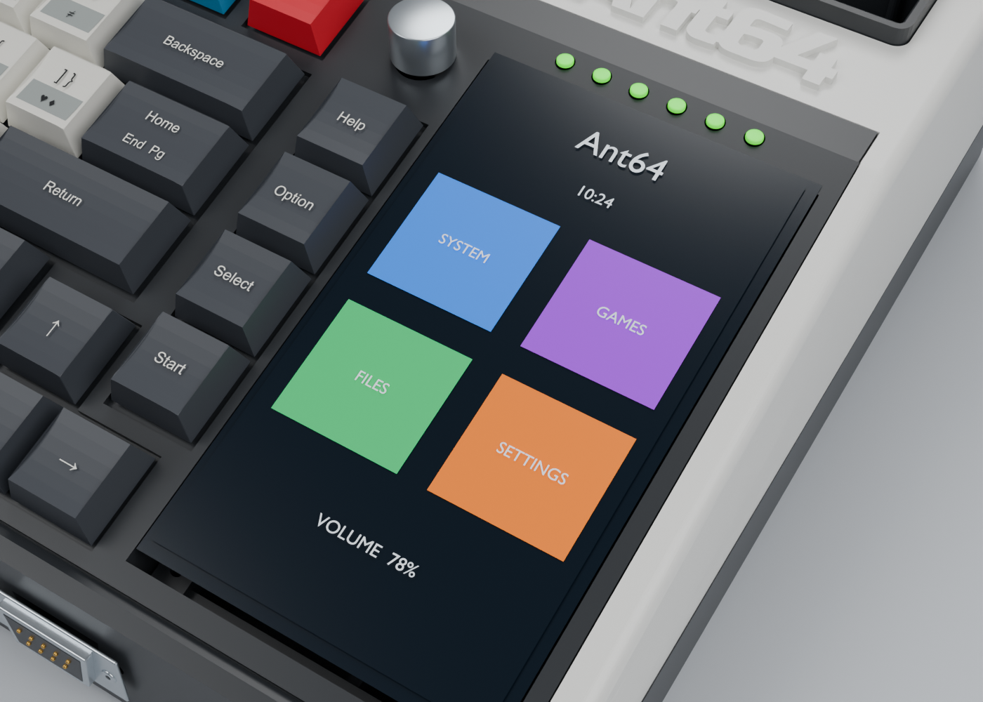
Concept visualisation of the touchscreen interface.
In addition to the HDMI feed into the FPGA, DeMon owns a 4.3″ portrait touchscreen where the numeric keypad would sit — a 480×800 IPS TFT (ST7102 controller, in-cell capacitive touch, 300 nits, 16.7M colour). The display is driven over a 4-lane MIPI DSI straight from the CM5; the touch reports over I²C on DeMon's housekeeping bus (touch reset on the MCP23017, PA5 — the panel also has a separate display reset, see below). Neither path depends on the FPGA being in a usable state.
Power and signal levels (from the module's 30-pin FPC datasheet). The panel takes three supplies: VCC at 2.8 V (panel), IOVCC at 1.8 V (all digital I/O), and the backlight LED string (LEDA / LEDK×2) off a backlight driver (boost), its brightness set by the PWM pin. Every digital line is in the 1.8 V IOVCC domain — the touch I²C (TP_SDA/TP_SCL), touch interrupt (TP_INT), both resets (display RESET and touch TP_RESET), TE, and PWM. So the touch I²C crosses to DeMon's 3.3 V housekeeping bus through a bidirectional level translator (PCA9306-class, 1.8 V pull-ups off the IOVCC rail); the lines DeMon drives (the two resets, now on GP34/GP35) are shifted 3.3 V → 1.8 V, PWM is shifted 5 V → 1.8 V because it comes from Clicky PB2 rather than DeMon, and TE / TP_INT are shifted 1.8 V → 3.3 V back. The 1.8 V figures here are the bare-module case only — reference each translator's low side to the panel's own IO rail so a 3.3 V finished board drops in without a carrier change; see Reference every panel translator to the panel's own IO rail above. The MIPI DSI — four data lanes (D0–D3) plus clock — needs no shifting: D-PHY is its own defined differential signalling, PHY to PHY. (480×800 is modest, so it can run on fewer lanes if the CM's DSI brings out only two.)
| Group | Signals | Notes |
|---|---|---|
| Backlight | LEDA, LEDK×2 |
LED string — needs a backlight driver (boost); brightness via PWM |
| Supplies | VCC 2.8 V, IOVCC 1.8 V |
Panel rail + the 1.8 V I/O logic rail |
| Display control (1.8 V) | RESET, TE, PWM |
LCM reset (GP34), tearing-effect sync out (DeMon), backlight PWM in — PWM is Clicky PB2, not DeMon, so it can hold the panel dark from power-on |
| MIPI DSI | D0± D1± D2± D3±, CLK± |
4 data lanes + clock, differential — no shifting |
| Touch (1.8 V) | TP_SDA, TP_SCL, TP_INT, TP_RESET |
I²C + interrupt + reset |
| ID | LCM_ID |
Panel identification |
The display RESET is a second reset line beyond the touch reset on PA5: it sits on MCP23017 PA4 (shifted to 1.8 V), so both panel resets land on adjacent expander pins in the same 1.8 V group.
This matters because the touchscreen is visible at all times:
- At power-on, the FPGA loads its native Ant64 chipset from its own flash in a fraction of a second.
- During FPGA reload (personality cartridge swap, bitstream update, recovery), the main display blanks while the FPGA reconfigures — typically up to ~1 second for a full personality bitstream, a fraction of a second for a native-chipset reset. The touchscreen continues to show AntOS status, progress, and any interactive prompts throughout.
- During normal operation, the touchscreen is a secondary display surface — AntOS can render system status, the file browser, settings, debug info, soft keys, or jog-dial-style controls here.
Combined with Pulse's circular display above the keyboard (see Pulse), the Ant64 has two always-on auxiliary displays that survive any FPGA state — useful for diagnostics, recovery, and informational UI that needs to be visible even when the main display compositor isn't running.
Hidden Debug Display — SSD1363 OLED (optional)
DeMon optionally drives a small OLED (SSD13xx-class controller, I2C at 0x3C on the main bus) as a hidden diagnostic surface inside the case. The OLED is not fitted by default — it's a builder/developer option for units that need a permanently-on debug surface independent of the FPGA, MIPI, network, and keyboard touchscreen. Production Ant64s typically ship without it; debugging and development units, kits, and field-service builds may include it.
When fitted, the OLED is for the system to talk to itself — boot progress, subsystem state, scrolling event log, recovery information. It is read by whoever opens the case or knows where to look, not by users in normal operation. Unlike the keyboard touchscreen (which is user-facing and shows AntOS UI), the OLED is purely for introspection.
The OLED's value is its independence. It runs on plain I2C from DeMon and comes alive within milliseconds of power-on — before the FPGA loads, before MIPI is configured, before the network is up, before the user touchscreen has initialised. If any of those subsystems is itself the thing that's broken, the OLED still tells the story.
When not fitted, sys_oled detects no device on the bus and silently disables itself — all the diagnostic content that would have gone to the OLED still goes to the UART console and (once available) the network debug stream, so nothing is lost functionally. The OLED is purely additive.
Full layout, screen list, and refresh strategy are documented separately in Debug Display.
Smart Cart — Cartridge Port
A 30-pin edge connector connected to DeMon (one of the hub USB DP/DN pinouts, the C: drive) and of the spare pins on the chips. The full pinout, the physical notes, and the catalogue of cartridge designs (ICP, chain cart, …) live in Cartridges.
- If a cart is present at boot, it is used in preference to the A: SD card
- Cart insertion/swap whilst powered on triggers an automatic reboot (can be disabled)
- Cart can be safely removed whilst powered on — no reboot
- Reinserting the same cart also does not reboot
Built-In NFC Card Reader
The Ant64 has an on-board PN532 NFC reader — no cartridge required. Its antenna sits just behind the cartridge port, so a card placed at the cartridge slot is read directly: the same physical location accepts either a cartridge or a tapped NFC card.
The reader is on Clicky's dedicated NFC I²C bus (Clicky is the I²C master), with reset and IRQ on Clicky — moved off DeMon's housekeeping bus so NFC has its own I²C. Clicky handles the whole low-level stack — card types, NDEF, validation — and hands DeMon a clean, validated card record over I²C (its slave interface at 0x28); DeMon keeps the higher-level card model — the "a card is a URL" scheme-dispatch mechanism, user/environment (DBFS) switching, and the game-manifest system, documented in NFC — Cards, DBFS Switching & the Game Manifest System (see also Clicky → NFC Reader). A card carries only a short URI (a manifest URL or a dbfs:// target); game content is cached in the user's DBFS rather than on the card.
Neopixels — 8 Status LEDs
These eight WS2812 status LEDs are still controlled by DeMon, but physically driven by Clicky. DeMon sends a per-LED colour/state intent to Clicky over I²C and Clicky drives the string; the buzzer works the same way — DeMon tells Clicky which tone to play and for how long, and Clicky handles the timing. DeMon never bit-bangs LED or buzzer timing itself. (Latency-critical key events come the other way, over UART — see Clicky.)
| No. | Name | Behaviour |
|---|---|---|
| 0 | Power | Off → white (self test) → amber (booting) → green (ready) |
| 1 | External SD card | Off / blue (detected) / green (R/W) / red (error) |
| 2 | Cartridge SD | Off / blue (detected) / green (R/W) / red (error) |
| 3 | Main (fast) SD | Off / blue (detected) / green (R/W) / red (error) |
| 4 | Network | Off / blue (connected) / green (R/W) / red (error) |
| 5 | Wi-Fi | Off / blue (connected) / green (R/W) / red (error) |
| 6 | Bluetooth | Off / green (R/W) / red (error) |
| 7 | MIDI | Off / green (R/W) / red (error) |
During self-test all LEDs go white, then change individually: green = passed, red = failed. LED functions are documented and can be repurposed if needed.
Power and the power button
Power is supplied by USB-C, in via a one-way diode (1N5822?). The soft power switch is owned by Clicky — Clicky senses the button and drives the power-off line (moved off DeMon's MCP23017), because it is always alive on the switched 5 V rail. DeMon receives the power-button press via KINT + an I²C status read and, after a graceful AntOS shutdown, commands Clicky over I²C to cut power; a ~10 s button hold makes Clicky force power down directly, even if the CM5 is wedged.
Sparkfun open source soft power switch mk2
What DeMon Can Reprogram
- FireStorm FPGA bitstream (via JTAG) — without interrupting AntOS
- FireStorm FPGA flash (via JTAG chain)
- Pulse (via USB-Serial-JTAG, through DeMon's FS hub)
- Sticky (via UPDI through Pulse)
- Cranky (via UPDI through Pulse)
- Clicky keyboard controller (via UPDI through Pulse — serialUPDI over UART4)
- ESP32-C5 (via USB-Serial-JTAG, through DeMon's FS hub)
DeMon's OS is re-imaged by rewriting its SD card. Because AntOS lives on DeMon, re-imaging is a deliberate, deeper-recovery operation — it reboots the OS. Recovery is layered: the card's recovery slot can re-flash the OS slots in place, and the floor is re-imaging the removable card from a PC; if the FPGA side is bricked, JTAG access from a PC can rebuild FireStorm from scratch.
If anything goes wrong — Ant64 can heal itself.
Storage
The Ant64 has a layered storage topology, hosted off DeMon's USB controllers. Throughout this section, internal drives sit inside the case (not user-removable in normal use) and external ports are sockets mounted on the case, accessible from outside without opening the box.
Drive-letter assignment is port-based — each physical USB port maps to a fixed letter, independent of attach order or enumeration timing. The complete drive-letter scheme, DBFS shadowing rules, multi-user DBFS support, and boot/hot-plug behaviour are documented in Filesystem & Drive Letters.
USB topology — HS storage hub, FS HID hub
DeMon's two USB 2.0 OTG controllers are split by role:
- HS USB OTG → storage hub. The High-Speed port drives a hub carrying up to four USB mass-storage devices, run at High-Speed for bulk throughput:
- D: — DBFS master — primary storage for AntOS, applications, user data, the DBFS database
- D!: — DBFS shadow — a continuous mirror of D: for redundancy; hidden from user-facing APIs; if the primary drive fails, no user data is lost — the shadow takes over
- B: — Internal general drive — additional internal storage for things that don't belong in DBFS (large media libraries, downloaded asset caches, OTA staging)
- C: — cartridge port — user-supplied cartridge
- E: — External memory-stick port — user-supplied USB memory stick for transient data, transfers, and backups
- FS USB OTG → HID hub. A Full-Speed hub carries the human-interface and debug devices:
- Keyboard and mouse
- ESP32-C5 USB-Serial-JTAG — program / debug of the radio companion
- Pulse USB-Serial-JTAG — so DeMon programs / debugs Pulse (Pulse's own OTG ports are committed: HS to FireStorm, FS to its MIDI port)
Drive-letter assignment is port-based on the storage hub (see Filesystem).
External SD card slot
An external SD card slot (mapped as A:) for user-supplied removable storage, it used the SDIO0 lines on the CM5, so it should be much faster than SPI mode — used by the MOD player, sample import, Doom WAD libraries, save transfers, and as a generic file source for AntOS. It is not the primary system storage (DBFS holds that on D:); the slot is for removable media and bulk content.
Prototype
The prototypes use the CM4 lite (eZXSpectrum, user swappable to CM5 lite) on one board (the CM4 RPi I/O base board) and a CM5 lite (Ant64) on another board (the CM5 RPi I/O base board).
Reference Links
Related AntOS docs: bringup (CM5 bring-up, firmware corrections, integration ladder) · os_card (partition layout, config.txt, EEPROM config) · firmware (A/B update flow, recovery ladder) · cm45 (CM-supervisor design notes).